AI Technical Articles
OpenAI’s AI Chip Design Results: What the 14% Claim Means
OpenAI’s reported chip-design results are significant, but not because an AI independently designed a better processor.
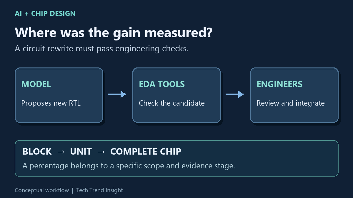
The more precise finding is that AI models can act as search partners for chip engineers. They propose alternative circuit implementations, while established engineering tools check behavior and estimate power, performance and area. These checks provide evidence within their tested conditions; they do not make every generated circuit correct. Engineers then decide which candidates can proceed.
That distinction matters when interpreting OpenAI’s headline result. The company’s November 18 announcement reports up to 14% PPA improvement on heavily optimized AMD graphics-processing-unit (GPU) circuit designs, and says some model-written changes entered a design sent for manufacturing. However, OpenAI has not publicly provided enough underlying design and verification data for outsiders to independently reproduce that production result.
So what did the AI actually do?
Three terms make the claim easier to understand
RTL, or register-transfer level, is a description of how digital circuitry behaves and moves data between registers. A register holds a value between clock ticks, and RTL describes when values move or calculations occur. SystemVerilog is one language engineers use to express RTL. In this work, OpenAI says its models generated and rewrote RTL for circuit blocks.
EDA, or electronic design automation, refers to software used to synthesize, simulate, analyze, and verify chip designs before fabrication. OpenAI says it coupled its models with Synopsys tools to evaluate candidate designs.
PPA means power, performance, and area. Power is electrical consumption, performance concerns how quickly useful work completes, and area is the circuit’s silicon footprint. These objectives can trade off against one another: a circuit that runs faster might consume more power or occupy more silicon. PPA is a group of objectives, not a universal single score. The headline does not establish a 14% improvement in each of the three, nor a 14% faster complete GPU. Interpreting it requires the objective, constraints and measurement method. Synopsys provides an overview of PPA and these trade-offs.
The AI proposes; the engineering loop decides
The process OpenAI describes is closer to automated design exploration than autonomous chip creation.
In simplified form:
- Engineers provide an existing RTL design, requirements, tests, and constraints.
- The AI model proposes another RTL implementation.
- EDA tools synthesize, simulate, and evaluate the candidate.
- Candidates that fail correctness tests or engineering constraints are rejected.
- Engineers review surviving designs before later physical-design and manufacturing stages.
Simulation runs selected inputs through a design and compares the outputs with expectations. Equivalence checking asks whether a rewrite preserves the specified behavior of the original; its coverage depends on the model and assumptions used. Neither a short test suite nor an attractive area estimate is a substitute for the project’s complete verification process.
The crucial point is that plausible-looking SystemVerilog is not enough. A proposed implementation must survive conventional verification and engineering evaluation.
OpenAI describes this iterative combination of model-generated RTL and EDA evaluation in its chip-design report.
Jalapeño shows what an “improvement” can actually mean
One of OpenAI’s clearest examples comes from Jalapeño, its processor project.
OpenAI reports that a model-generated redesign of a multiplier in Jalapeño’s matrix-computation unit used approximately 15% less standard-cell area after synthesis while reducing latency from two clock cycles to one. It separately reports an adder redesign with an approximately 15% area reduction while retaining two-cycle latency.
Those percentages apply to individual circuit blocks, not the entire processor.
“In synthesis” is also an important qualification. Synthesis translates RTL into a network of standard cells: the library building blocks used to implement logic. Its cell-area estimate is not the complete die footprint, which also depends on components and physical-layout requirements outside that estimate. It is not equivalent to measuring the size, power, or performance of a complete fabricated processor.
OpenAI reports evidence at a later stage for accumulated Jalapeño optimizations. It says model proposals reduced standard-cell area by about 13% in the vector unit and 10% in the matrix unit, with those optimizations subsequently demonstrated during silicon bring-up.
That is a much more informative description than simply saying AI “designed a chip.”
A worked example: smaller part, smaller total gain
Assume a hypothetical design has 100 square millimeters (mm²) of standard-cell area, including a 20 mm² multiplier block. If only that block shrinks by 15%, it saves 3 mm²: 20 × 0.15 = 3. The total becomes 97 mm², a 3% reduction. This example holds every other cell area fixed and excludes layout and other die-area effects; it is not a calculation of Jalapeño’s savings.
The same scope check applies to clock cycles. A clock cycle is one tick of the circuit’s timing rhythm. At a fixed 2-nanosecond cycle time, two cycles take 4 nanoseconds and one takes 2. If the redesigned circuit needs a longer cycle, the elapsed-time improvement changes. Fewer cycles in one multiplier also do not establish twice the throughput of a whole processor, which must feed that block with data and complete other work.
What does the AMD “up to 14%” result establish?
The AMD claim has stronger production relevance, but less public detail.
OpenAI reports up to 14% PPA improvement over heavily optimized baselines on flagship AMD GPU IP (intellectual property: reusable circuit designs). It also says some model-generated changes were incorporated into a recent design sent for manufacturing, while other changes entered production design files for possible use in later versions.
OpenAI additionally reports single-digit PPA improvements on important blocks of an upcoming AMD CPU.
These are meaningful claims about work close to production, but they should be described as OpenAI-reported collaboration results, not benchmarks independently reproduced by this publication.
The public material does not provide enough block-by-block data to determine how power, performance, and area individually contribute to the headline 14% result, nor does it disclose the production RTL and complete verification evidence needed to reproduce it independently.
“Sent for manufacturing” also should not be confused with a result demonstrated on working silicon. It indicates that the design has progressed substantially further than a synthesis experiment, but it is a different evidence stage from testing a fabricated part.
That distinction separates the AMD result from OpenAI’s reported silicon-bring-up evidence for Jalapeño.
Open-source processor tests show both the promise and the limitations
OpenAI also tested generations of its models on two open-source 32-bit RISC-V processor cores (RISC-V is an instruction-set architecture: the rules defining the instructions a processor executes), PicoRV32 and Ibex.
In the reported evaluation, candidates received a score of zero if they failed simulation tests or exceeded 16 times the original core’s area. Designs that passed were then evaluated on hidden workloads using an estimated throughput score.
The important result is not that these experiments produced an autonomous replacement for a production CPU team. Rather, they show that a model can repeatedly generate hardware implementations and search a design space when automated tests provide feedback.
OpenAI also describes a significant limitation: when models generated processors from written requirements, they could omit features such as performance counters or additional instructions. The company says tighter area constraints and physical-synthesis timing checks would make the evaluation more representative of production chip development.
That gap matters. Passing a benchmark under a bounded specification is not the same as taking a complete modern processor specification through verification, physical design, sign-off, and fabrication.
How to read future “AI-designed chip” claims
Instead of asking whether a chip was “designed by AI,” four questions make such announcements easier to evaluate.
What did the model produce?
Generating advice, RTL, a physical layout, and verification evidence are very different accomplishments.
In OpenAI’s examples, the central model output is RTL.
What established correctness?
A circuit is not correct because a language model generated it. Look for evidence such as simulation, equivalence checking, formal verification, physical-design checks, or testing of manufactured silicon.
Check what was compared, which inputs or properties were checked, and whether any constraints changed. A faster candidate that silently drops a required instruction has changed the task.
Where was the improvement measured?
A 15% area reduction in one multiplier is not a 15% reduction in the area of a processor.
The relevant denominator might be a circuit block, functional unit, processor core, or complete chip. Without that scope, a percentage can sound much more consequential than it actually is.
How far did the design progress?
A useful evidence chain is:
model proposal → synthesis estimate → physical verification and sign-off → manufacturing → working silicon
Evidence becomes more consequential as a design advances through that chain. Results from one stage should not be presented as though they had already reached the next.
What to take from the result
The useful advance is that model-written circuit changes have reached production design work, according to OpenAI. That gives engineers another way to explore implementations, while leaving correctness checks and physical engineering essential.
For a team evaluating this approach, start with a bounded block whose required behavior and baseline are explicit. Compare candidates under the same tool settings and constraints, retain failed candidates in the evaluation record, and require the usual verification before integration. For a reader assessing the announcement, ask for the block, the denominator and the evidence stage before translating a percentage into a claim about a complete chip.